series resonant circuit magnitude of Xl is equal with magnitude of Xc. Therefore, impedance
decreasing and current increasing.

ωL = 1/ωC , ω0^2 = 1 / (LC) , 2πfo = ω0 , fo is resonant frequency of a series circuit. Under resonant
Average power at resonant frequency is P(avg) = (Vm)^2 / (2R) .
At a certain frequencies ω = ω 1 , ω 2 , called the half-power
frequencies the dissipated power is half the maximum value.
P(ω1) = P(ω2) = (Vm/radical(2))^2 / 2R = (Vm)^2 / (4R) . ω02 = ω1* ω2
B is a half-power bandwidth B = ω 2 −
ω 1
Q = 2(pi) (peak energy stored in the circuit)/(energy dissipated by the circuit in one period at resonance)
The quality factor of a circuit in resonant: Q = (ωoL)/R , B = R/L = ωo / Q
| Changes of Q Relative to Resistance |
High-Q circuits are used
often in communications networks.
ω1 ≈ ωo - (B/2) , ω2 ≈ ωo + (B/2)
Parallel Circuit resonant
In contrast with a series circuit, in parallel circuit impedance is maximum and current is minimum.


A filter is a circuit that design to select a specific frequency and reject others.
1. A low-pass filter (LPF) passes low frequencies and stops high
frequencies.
 |
| A Low pass RC Circuit |
Transfer function for a RC series low pass filter.

When f is low, XC is high and Vc = Vout is maximum. When f is high, XC is minimum
and Vc = Vout is minimum.

When f is low, XL is low and VR = Vout is maximum. When f is high, XL is maximum
and VR = Vout is minimum.
2. A high-pass filter (HPF) passes high frequencies and rejects low
frequencies.
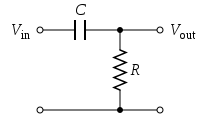

When f is low, XC is high and VR = Vout is minimum. When f is
high, XC is minimum and VR= Vout is maximum.

When f is low, XL is low and VL = Vout is minimum. When f is
high, XL is maximum and VL = Vout is maximum.
3. A band-pass filter (BPF) passes frequencies within a frequency
band and blocks or attenuates
frequencies outside the band.
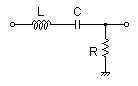 This is a series RLC circuit. In resonant frequency Z = R and current is
maximum so VR = Vout is also maximum.

4. A band-stop filter (BSF) passes frequencies outside a frequency
band and blocks or attenuates
frequencies within the band
.
This is a series RLC circuit. In resonant frequency Z = R and current is
maximum so VR is maximum, and Vout is minimum.


