Bipolar Junction Transistor (BJT) is a Semiconductor device constructed with three
doped Semiconductor Regions (Base, Collector, Emitter) separated by two p-n Junctions,
The p-n Junction between the Base and the Emitter has a Barrier Voltage (V0) of
about 0.6 V, which is an important parameter of a BJT.
 |
| Figure 1: A NPN BJT Schematic Symbol |
 |
| Figure 2: A PNP BJT Schematic Symbol |
Typically, the emitter region is heavily doped compared to the other two layers, whereas the majority charge carrier concentrations in base and collector layers are about the same. A cross section view of a BJT indicates that the collector–base junction has a much larger area than the emitter–base junction.
 |
| Figure 3: A Cross Section of a Planar NPN BJT |
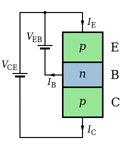
.Charge flows in a BJT is due to diffusion of charge carriers across a junction between two regions of different charge concentrations. IE = IB + IC , VCE = VCB + VBE
 |
| Figure 4: NPN BJT with forward-biased E–B junction and reverse-biased B–C junction |
In order a bipolar junction transistor works at its active region, the base-emitter junction must be in forward biased, and the base–collector junction must be in reverse biased.
 |
| Figure 5: A Schematic Connection of a PNP |
 |
| Figure 6: A Schematic Connection a NPN |
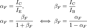
The common-emitter current gain is represented by βF or the h-parameter hFE; it is approximately the ratio of the DC collector current to the DC base current in forward-active region. It is typically greater than 50 for small-signal transistors but can be smaller in transistors designed for high-power applications.
Another important parameter is the common-base current gain, αF. The common-base current gain is approximately the gain of current from emitter to collector in the forward-active region. This ratio usually has a value close to unity; between 0.980 and 0.998. It is less than unity due to recombination of charge carriers as they cross the base region.
Alpha and beta are more precisely related by the following identities (NPN transistor):
There are three kinds of connection in a transistor according to its common terminal between input and output.
1) Common-Base (CB) 2) Common-Emitter (CE) 3) Common-Collector (CC)
In this lab a common emitter are used. The goal is graph of its output characterisitc.
The output current Ic is a function of the output voltage V(CE) and the input current IE.

A stair-step waveform with five levels is connected to the base by a 100k resistor. Each step is 5 ms and its height is 1 volt. So period is 25 ms, and each step has voltage levels (0.5 ,1.5 , 2.5 , 3.5 , 4.5). A symmetric triangle waveform is connected to the collector by a 100 ohms resistor. Its height is 5 v and its period is 5 ms (Fig 7).
 |
| Figure 7: Stair-Step Waveform & Triangle Waveform |
 |
| Figure 8: Output Characteristic of a NPN |
IC(1) = 0 , IC(2) = 1.9 mA , IC(3) = 4 mA , IC(4) = 6 mA , IC(5) = 8 mA
According to the fig 7:
Vavg(1) = 0.5 v , Vavg(2) = 1.5 v , Vavg(3) = 2.5 v , Vavg(4) = 3.5 v , Vavg(5) = 4.5 v
IB = (Vawg - V(BE)) / 100k , β = IC / IB , V(BE) = 0.7 v
IB(1) = (0.5 - 0.7) / 100k = 0 , IB(2) = (1.5 - 0.7) / 100k = 8 μA
IB(3) = (2.5 - 0.7) / 100k = 18 μA IB(4) = (3.5 - 0.7) / 100k = 28 μA
IB(5) = (4.5 - 0.7) / 100k = 38 μA
Questions:
β(1) = 0 , β(2) = 1.9 / 0.008 = 237.5 , β(3) = 4 / 0.018 = 222.2 , β(4) = 6 / 0.028 = 214.3 , β(5) = 8 / 0.038 =210
According to the figure 8 the slope of the fifth line is calculated.
Two points on the graph collector current vs emitter-collector voltage (0.5 v , 8 mA) & ( 4 v , 8.2 mA)
m = (8.2 - 8) / (4 - 0.5) = 0.057 (mA / v)
IC - 8 = m (VCE - 0.5) , IC = 0.057*V(CE) + 7.972 , If IC = 0 , V(CE) = V(A) , V(A): early voltage
V(A) = -7.972 / 0.057 , V(A) = - 139.9 v
β*V(A): The Beta Early Voltage. (210)*(139.8) = 29379
According to the figure 8 the slope of the forth line is calculated.
Two points on the graph collector current vs emitter-collector voltage (0.5 v , 8 mA) & ( 4 v , 8.2 mA)
m = (8.2 - 8) / (4 - 0.5) = 0.057 (mA / v)
IC - 8 = m (VCE - 0.5) , IC = 0.057*V(CE) + 7.972 , If IC = 0 , V(CE) = V(A) , V(A): early voltage
m = (8.2 - 8) / (4 - 0.5) = 0.057 (mA / v)
IC - 8 = m (VCE - 0.5) , IC = 0.057*V(CE) + 7.972 , If IC = 0 , V(CE) = V(A) , V(A): early voltage
V(A) = -7.972 / 0.057 , V(A) = - 139.9 v
According to data sheet hfe (IC = 10 mA , V(CE) = 1.0 vdc is between 100-300
The 2N3904 is common general-purpose low-power NPN transistor used amplifying or switching applications. It is typically used for low-current, medium voltage, and moderate speed purposes. This transistor is popular among hobbists and in academia and is arguably one of the most well-known general-purpose transistors in the world. The complementary or PNP version of the 2N3904 is the 2N3906. This general-purpose transistor is available in various packages, including through-hole (TO-92) and surface mount ( SOT-23 and SOT-223).
No comments:
Post a Comment